emmiTM Photoemission Microscopy:
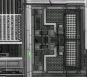
QFI owns the original patent on the photoemission technique; emmiTM is a trademark on QFI’s photoemission microscopy systems. Photoemission solutions are targeted at detecting and localizing gate leakage, dielectric breakdown, forward bias junction, oxide pinholes, and many other failures, which result in electron-hole recombination. Highly sensitive, very low noise sensors (cameras) capture small particles of light (photons) created during this electron-hole recombination. The emmiTM process includes the capture of a reflected mode (reference) image of the DUT. Then, illumination is turned off, and an emission mode image captures the photoemission events. The reference image and emission image are overlaid to highlight the location of emission sites on the DUT.

QFI is Known for High Quality, High Sensitivity Photoemission Images - Derived from Proprietary Sensor, Software, and Optics Designs
One of the earliest techniques utilized in IC failure analysis was static photoemission. As photoemission in silicon is a weak process, sensors must be highly sensitive and very low noise. Theses sensors are cooled to decrease noise and increase sensitivity. A low noise sensor is necessary to capture weak emissions, which can sometimes require long integration times of several minutes duration. Requirements for inspection from the backside of semiconductor devices necessitate sensors that detect in the near infrared (NIR) spectral range. This is because Silicon substrates are transmissive to light wavelengths beyond 1064 nm. Substrate doping leads to scattering and absorption of the light. Photoemissions are isotropic events. Thus, the same defect mechanisms that create photoemission from the front side of a semiconductor device will lead to photoemission from the backside of the device. Substrates can be thinned and polished to improve transmission from the backside of the DUT. Sample preparation tools are readily available in the market.
Requirements for static emission sensors depend on a complex combination of failure type, supply voltage, front or backside imaging, etc. QFI’s emmi™ line of photoemission sensors offers a range of choices to meet the user’s specific requirements. It should be noted that high Quantum Efficiency (QE) is an important characteristic of a quality emmiTM sensor. However, without consideration of signal-to-noise performance, QE can be misleading. Specific attention must be paid to application requirements in selecting the best combination of sensors.
QFI offers several photoemission sensors/solutions:
- VisNIR-1024 (deep depletion CCD for front side and backside applications—highest overall sensitivity)
- NIR-SWIR-320 (TE cooled InGaAs—added sensitivity for extended wavelength photoemissions)
- NIR-SWIR-256 and NIR-SWIR-640 (LN2 cooled InGaAs—maximum sensitivity for extended wavelength photoemissions)
- VisVNIR-512 (Frame Transfer CCD—high sensitivity front side inspection)
- VisNUV-1024 (High sensitivity visible and NUV photoemissions)
- EM-128 (electron multiplication CCD—for high speed photoemission—2000 frames/per second)
- Discrete filter full image frame spectral photoemission
- High-resolution single point photoemission spectroscopy
You are welcome to request additional information via the information request link:
